CEMOP is equipped with several high-level thin films and devices processing and characterization labs, including a clean room with a total area of 300m2; non-fab/printing lab and two characterization laboratories, with a total area of about 350m2. Moreover, through the collaboration existing with CENIMAT/I3N, four more laboratories are accessible dedicated to: thin film processing by solution; nanomaterials synthesis and biosensors; structural and optical characterization;and microscopy and surface analysis
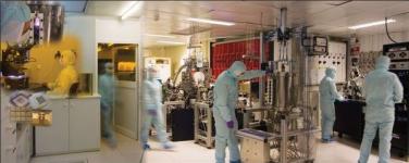
Clean Room Lab
Lab responsible:
Luís Pereira (ext. 13753)
Description:
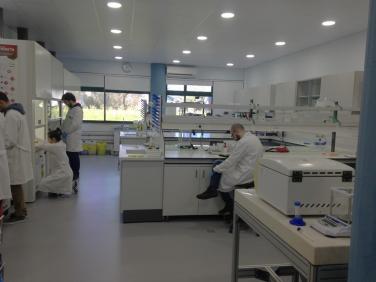
The thin-film deposition area is an ISO 7 lab devoted to the preparation of thin films by physical and chemical vapor deposition techniques, as required to fabricate micro/nanoscale devices.
The lab is equipped with a wide range of physical and chemical vapor deposition tools to fabricate a variety of thin film materials, such as metals, (transparent) conductors and semiconductors and insulators, with nm-thickness control. Most systems can accommodate up to 6” wafers. Tools include 5 sputtering, 2 plasma-enhanced chemical vapor deposition (PECVD), 4 evaporation and 1 CVD (parylene coater) systems. A rapid thermal processing (RTP) tool is also available for post-deposition treatments of thin films. A plasma-enhanced atomic layer deposition (PEALD) system with a glovebox for substrate loading/unloading in controlled environment.
Electrical characterization Lab
Lab responsibles:
Pedro Barquinha and Rui Igreja (ext. 11605)
Description:
The electrical characterization lab (1.03 CEMOP) is a space devoted to the evaluation of electric, dielectric and electrochemical properties of materials and devices.
This lab is equipped with multiple manual probe stations and semiconductor parameter analyzers for I-V, C-V, pulsed-IV and time-dependent measurements (e.g. bias stress), from cryogenic temperatures to 300 °C. It also includes potentiostats for electrochemical studies, hall-effect systems and cryogenic chambers with electrometers for analysis of carrier transport in materials. The laboratory is also fully equipped to analyze dielectric materials and sensors, with lock-in amplifiers, spectroscopic impedance analyzers and an RLC bridge. Several oscilloscopes, power supplies, wave generators and high-power LEDs with several wavelengths are available for customizable measurement setups. Finally, in a separated area of the lab a last-generation X-ray and Ultraviolet Photoelectron Spectroscopy (XPS/UPS) tool is installed for chemical and electronic characterization of materials.
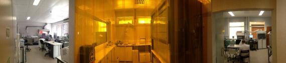
FunPaper Lab
Lab responsibles:
Luís Pereira (ext. 11617) and Diana Gaspar (ext.13747)
Description:
The FunPaper lab is a multidisciplinary lab that allow the development of new concepts and ideas for paper electronics.
This lab has three distinct areas. The first one is equipped with one chemical lab with a working station and lab equipment for manipulation of different materials and ink development, it also has a screen stencil printer, fully automated for mass-manufacturing of printed devices, two office printers, adapted for different inks and devices, a centrifuge and a extruder. The second area is a yellow zone, for handling of UV-sensitive materials and inks. The third area is a production area, dedicated to paper electronics technology, for the production of low cost flexible devices, using different deposition methods, such as a flexoprinter, two piezoelectric inkjet printers, a multicoater with interchangeable heads (dip coating, spray coating, electrospinning and inkjet printing), a spray pyrolisis equipment for large-area manufacturing of devices, two different shear casting equipments, with heated and magnetic beds, a viscometer for measuring ink viscosities, a sonicator, with two interchangeable tips, for suspensions, particle dispersion, homogenization, etc. and a table-top vacuum packaging machine.
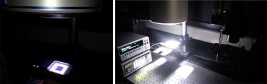
Nanophotonics and Energy Lab
Lab responsibles:
Manuel João Mendes (ext. 13742) and Hugo Águas
Description:
The lab 2.20 in CEMOP is a dark room assigned to opto-electronic measurements, mainly dedicated to the characterization of photovoltaic devices.
The lab is equipped with three solar simulators and two spectral response (i.e. quantum efficiency) systems, as well as installed air extraction, air conditioning and compressed air flow.
Chemical Lab
Responsible: Alexandra Gonçalves (ext. 11617)
Description:
The chemical lab is equipped with 3 microwaves synthesizers for performing a wide range of inorganic oxides nanoparticles such as ZnO, TiO2, IrO2 and Er2O3.
This lab has also 3 spin coaters to develop thin films used to produce different types of devices. In order to prepare the samples surfaces, the chemical lab is equipped with a UV ozone system integrated with an ozone elimination system.
The lab is equipped with all facilities for the synthesis and development of colloidal suspensions and nanoparticles generated in aqueous suspension.
Thin Film Lab
Lab responsible:
Alexandra Gonçalves (ext. 11617)
Description:
The thin film lab is a multidisciplinary lab that allow the development of new concepts and ideas.
This lab has three distinct areas. It is equipped with one chemical lab with a microwave synthesizer equipment to produce nanoparticles of different materials, a production area with two laser systems to cut, engrave and process different type of polymeric materials, several ovens and furnaces, a sputtering system and a thermal evaporator system to develop thin films. The third area is dedicated to lab-on-paper technology for the production of low cost biosensors and digital microfluidics and as also two 3D printer for the development of prototypes and to support the ongoing projects.
Processing Lab
Description:
This lab is dedicated to the processing of ceramic materials, glasses, metals and composites.
It contains several electrical furnaces that are used in the production of metal and in different heat treatments. It contains mixing equipment, hydraulic pressing machines and several electrical furnaces (kilns and tubular furnaces up to a temperature of 1500ºC) that are used in the sintering of the ceramic powders, preparation of glasses by melting and in different heat treatments. It is equipped with one 3D printer for the development of prototypes and to support the ongoing projects.
Nanofabrication Lab
Description:
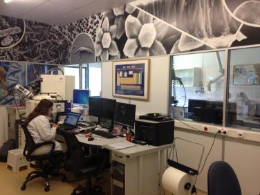
This laboratory is equipped with a Scanning Electron Microscopy Focused Ion Beam (SEM-FIB) workstation, Atomic Force microscopy unit, confocal microscope and a tabletop microscope. It has also a contact angle instrument for automated video contact angle metrology and drop shape analysis, 2 profilometers that measure roughness and step height, optical microscope and optical stereo microscope.
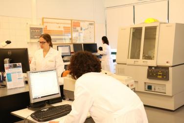
Characterization Lab
Lab responsibles: Alexandra Gonçalves (ext. 11617)
Description:
The characterization lab is equipped with several equipments such as XRD, FTIR, Raman Microscopy, DSC-TG, UV-Vis_NIR spectrometer, luminescence spectrometer, spectroscopic ellipsometer, microplate reader and sun simulater.