Characterizing the CEMOP/UNINOVA Infrastructure
The Center (CEMOP) is specially equipped for Research & Development, service providing and training activities in five main areas:
- microelectronic and optoelectronic devices' conception/production technologies and processes;
- tribologic and optic coatings;
- system project and conception;
- material and device characterization;
- and also device simulation/modeling.
In pursuit of its objectives, CEMOP takes part in several research projects, both fundamental and applied, involving universities, institutes and companies, both National and International. CEMOP's privileged partner for R&D related activities is the Center for Materials' Research of the FCTUNL (CENIMAT), with whom it cooperates on a regular basis.
Main Activities
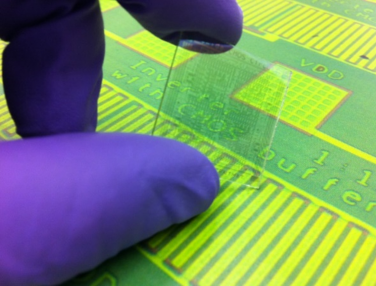
Semiconductor, transparent conductive oxide, semiconductor/oxide alloy and new welding metallurgic system's development and processing.
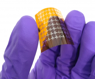
Solar cell development and processing; position sensors; gas sensors; infrared detectors; image sensors; non volatile memory systems; high permittivity and lateral area mini and micro capacitors; color sensors; thin film transistors; MOS and TTL devices; new micro-welding processes.
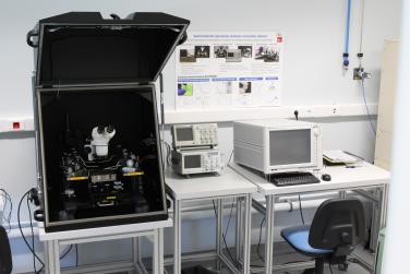
Material and device characterization, modeling and simulation.
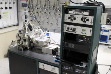
Project and conception of repair/maintenance technical assistance systems for vacuum systems (clean rooms); photovoltaic system dimensioning; development and production of industry pre-production and prototype units, in the above stated areas.